With the continuous evolution of microelectronics packaging technology, the power density of electronic components has increased significantly, resulting in a sharp increase in heat generation per unit volume, which has put forward more stringent standards for the performance of the new generation of circuit boards in terms of heat dissipation efficiency (thermal conductivity). At present, researchers are actively exploring and developing several ceramic substrate materials with high thermal conductivity, including aluminum nitride (AlN), silicon carbide (SiC) and beryllium oxide (BeO). However, BEOs are environmentally limited due to their potential toxicity; SiC is not considered an ideal substrate material due to its high dielectric constant. In contrast, AlN has become a high-profile choice of substrate materials due to its similar coefficient of thermal expansion to silicon (Si) and moderate dielectric constant properties.
Traditionally, thick film slurries have been mainly developed based on alumina (Al2O3) substrates, but the components of these slurries are prone to chemical reactions when in contact with AlN substrates and produce gas, which poses a serious threat to the stability and performance of thick film circuits. In addition, because the coefficient of thermal expansion of the AlN substrate is lower than that of the Al2O3 substrate, the direct use of the slurry and sintering process designed for Al2O3 on the AlN substrate will lead to thermal expansion mismatch, which will cause problems. Therefore, it is not advisable to simply transplant the material system and production process applicable to the Al2O3 substrate to the AlN substrate. This paper focuses on the fabrication process of resistors on AlN substrate, discusses the fabrication process deeply, and evaluates and analyzes the performance of resistors in detail.
resistance design number
In order to determine the relationship between the resistance value of AlN substrate and the number of design squares, the resistance test plate was designed (as shown in Figure 4). The length of the resistance ranges from 500 to 2000μm, and the width ranges from 500 to 2500μm. The resistors of four kinds of square resistance were printed on the AlN substrate, and the film was sintered at 850℃, and the resistance values of the resistors of different design sizes were measured.
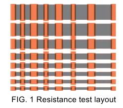
The resistance value of three substrates of the same size is measured, the design square number of the size resistance is calculated, the resistance value of the three resistors is averaged, and the relationship between the resistance value and the square number of the four kinds of square resistance is formed (as shown in Figure 2).
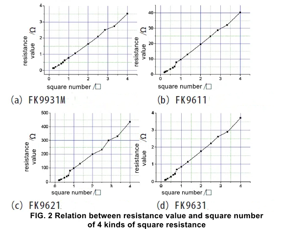
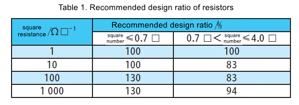
When the initial value of the resistance printing is generally designed to be 80% of the nominal value, it is most conducive to the improvement of the adjustment value and the yield. Combined with the relationship diagram between the resistance value and the square number, the design proportion of the four square resistors is calculated (see Table 1).
resistance value adjustment process
In the actual production of thick film resistance, even if the slurry composition, printing process, film thickness, firing, and electrode matching are strictly controlled, the error between the resistance value and the target value can only reach ±20%. In order to obtain the resistance value of the required precision on the basis of the thick film resistor that has been made, the value can only be adjusted. In terms of improving the precision of the yield and resistance value, value adjustment is an essential and important technology.
The process parameters of resistance adjustment on AlN substrate are as follows: current 14.5A, Q frequency 2500Hz, laser point distance 150. Based on the analysis of the shape of the cut marks after adjustment, the width of the resistance cut marks of the four kinds of square resistance is greater than 30μm, and there is no resistance and substrate debris in the cut marks, which meets the relevant requirements of the inspection documents.
In summary, with the rapid development of microelectronics packaging technology, the requirements for the heat dissipation efficiency of the circuit plate are increasing, which promotes the research and development of high thermal conductivity ceramic substrate materials. Among them, aluminum nitride (AlN) stands out among many candidate materials due to its superior thermal expansion matching and moderate dielectric constant characteristics, and has become a popular choice for a new generation of circuit board materials. However, the uniqueness of the AlN substrate also requires us to make corresponding adjustments and optimizations in the selection of thick film slurry and the production process to avoid the problems caused by the same material system and process as the Al2O3 substrate.
By designing the resistance test plate, measuring and analyzing the relationship between resistance and square number, and exploring the resistance adjusting technology, the resistance manufacturing technology on AlN substrate is deeply studied in this paper. The results show that the resistance with stable performance and high precision can be made on AlN substrate by designing the size ratio of resistance reasonably and controlling the process parameters precisely. These research results not only provide technical support for the application of AlN substrate in the field of microelectronics packaging, but also provide an effective solution for the heat dissipation problem of high power density electronic components in the future. With the continuous progress of technology, the improvement of the AlN substrate and its supporting production process will inject new vitality into the sustainable development of the microelectronics industry.