With the development of microelectronics packaging technology, the power and density of electronic components are increasing, and the heat per unit volume is increasing, and the requirements for the heat dissipation capacity (that is, thermal conductivity) of the new generation of circuit board are also more stringent. At present, the high thermal conductivity ceramic substrates developed are AlN, SiC and BeO. BeO is toxic and not conducive to environmental protection. The dielectric constant of SiC is too high to be used as substrate. AlN has attracted much attention because of its thermal expansion coefficient close to Si and moderate dielectric constant.
The traditional thick film slurry is developed based on the Al2O3 substrate, and its composition is easy to react with the AlN substrate and produce gas, which has a disastrous impact on the performance of the thick film circuit. In addition, the thermal expansion coefficient of the AlN substrate is lower than that of the Al2O3 substrate, and the traditional slurry sintered on the AlN substrate has the problem of thermal expansion mismatch. Therefore, it is not feasible to directly copy the material system and production process applied to the Al2O3 substrate to the production process of the AlN substrate. In this paper, the production process of resistance on AlN substrate is introduced, and the performance of resistance is studied.
Resistance Production Process Research
According to the recommended thickness of the resistance (12μm), the screen plate of the resistance is made of stainless steel mesh with a diameter of 75μm and the film thickness is 25μm. In the process of screen printing, the film thickness of the resistor can be adjusted by adjusting the printing parameters. There is a certain correspondence between the wet film, the drying film and the fired film. Through the adjustment of printing parameters such as pressure, printing speed, mesh spacing, the wet film thickness of the printing resistance paste can be controlled, and the film thickness tester is used to measure it, and the corresponding relationship between the wet film and the dry film can be corresponding after firing.
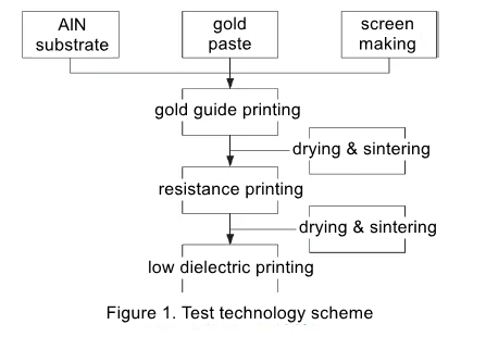
Gold conductor, resistance and low temperature medium are fabricated by thick film process (as shown in Figure 1). During printing, the wet film thickness of the resistance is controlled at 35μm. After the resistance is fired, the characteristics of laser adjustment, resistance temperature coefficient (TCR) and resistance stability are checked and verified.
Sintering Process Conditions
The resistance paste is composed of conductive phase, adhesive phase and organic carrier. In the sintering process, the bonding phase flows, and in the subsequent cooling process, it solidifies into a film, attaches to the surface of the ceramic substrate, and plays the role of bonding with the ceramic substrate and supporting the conductive chain. According to the recommendation of technical data, the resistance sintering process of AlN substrate is determined as follows: peak temperature 850℃, holding time 10min, and total sintering time 60min.
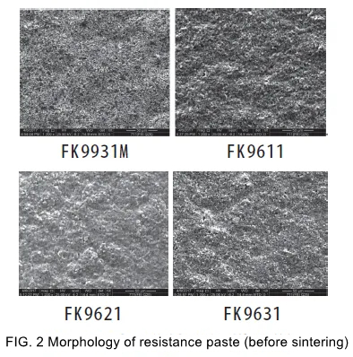
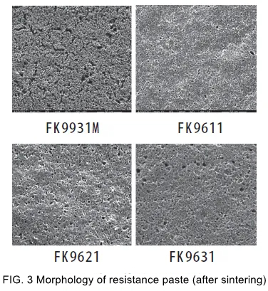
Figure 2 shows the appearance after printing of the resistance paste. At this time, the resistance film is formed by the loose ruthenium oxide (or palladium, silver) bonded under the action of organic resin with certain bonding force, and has an uneven surface. Due to the insulating effect of the binder, the resistance value of the resistance film layer is very large. During sintering, with the increase of sintering temperature, the organic components in the film gradually burn and volatilize (at 500℃, the organic adhesive is completely discharged), so that the ruthenium oxide particles are gradually pulled together and connected to each other to form a continuous conductive path. The morphology after resistance sintering is shown in Figure 3, and the film layer is obviously shrunk and densified after sintering.
In summary, with the continuous progress of microelectronics packaging technology, the heat dissipation performance of circuit board is increasingly required. AlN substrate has become a research hotspot due to its thermal expansion coefficient and moderate dielectric constant close to Si. However, the traditional thick film slurry and production process based on Al2O3 substrate can not be directly applied to AlN substrate, there are significant thermal expansion mismatch and reactivity problems. In this paper, the production process of resistance on AlN substrate is discussed deeply. By adjusting the parameters of screen printing, the thickness of resistance film is controlled, and the sintering process conditions are optimized, the production of resistance on AlN substrate is successfully realized. The research results show that the resistance with stable performance can be prepared through reasonable process control, which can meet the high requirements of heat dissipation and performance of the new generation of circuit board, and provide strong support for the development of microelectronics packaging technology.