The vigorous development of the semiconductor industry, as an important support for the progress of modern science and technology, continues to promote the exploration of miniaturization, higher speed and higher performance integrated circuits. This trend has directly led to a leap in the precision and technical difficulty of the semiconductor manufacturing process, and every minute link is highly dependent on advanced, high-quality and high-precision semiconductor manufacturing equipment. Silicon carbide (SiC), as an outstanding class of structural ceramic materials, shows extraordinary adaptability and stability with its excellent physical properties - high density, excellent thermal conductivity, amazing bending strength, high elastic modulus, excellent corrosion resistance and excellent high temperature resistance. It can effectively resist the extreme environment encountered during wafer processing such as epitaxial growth, etching and other stages, including strong corrosion and extremely high temperature conditions, and is not prone to stress deformation or thermal strain. Therefore, silicon carbide in a number of key steps in semiconductor manufacturing, such as fine grinding and polishing, epitaxial/oxidation/diffusion and other heat treatment processes, lithography technology, thin film deposition, precision etching and ion implantation, etc., have been widely recognized and applied, becoming an important force to promote semiconductor technology.
The etching process in semiconductor manufacturing uses plasma ionized by liquid or gas etchers (such as fluorinated gases) to bombard the wafer, selectively removing unwanted materials until the desired circuit pattern is left on the wafer surface. Thin film deposition is similar to the reverse process of etching, which uses the method of deposition to repeatedly stack insulating materials and cover each layer of metal to form a thin film. Since these two processes also use plasma technology and other technologies that are easy to cause corrosion to the cavity and components, the components in the equipment are required to have good plasma resistance characteristics and low reactivity and low conductivity to fluorine-containing etched gases.
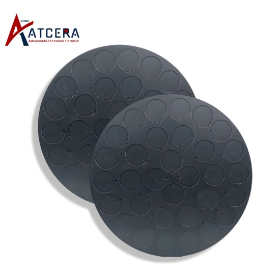
Traditional etching and deposition equipment components, such as focusing rings, are made of materials such as silicon or quartz. However, with the advancement of integrated circuit miniaturization, the demand and importance of integrated circuit manufacturing for etching process is increasing, and it is necessary to use high-energy plasma to precisely etch silicon wafers at the microscopic level, which provides the possibility to achieve smaller line widths and more complex equipment structures. Therefore, chemical vapor deposition (CVD) silicon carbide with its excellent physical and chemical properties. And high purity, high uniformity and so on have gradually become the first choice of etching, deposition equipment coating materials. At present, CVD silicon carbide parts in etching equipment include focusing rings, gas spray heads, SiC tray, edge rings, etc. In the deposition equipment, there are chamber cover, cavity lining, SiC coated graphite base, etc.