Silicon carbide, the emerging star of the semiconductor material industry, is gradually leading the innovation trend of microelectronics technology with its excellent performance indicators. Its unique thermal conductivity, far superior to traditional semiconductor materials, provides the possibility for efficient heat dissipation, especially in high-power electronic devices show unparalleled advantages. Coupled with its wide band gap characteristics, the silicon carbide substrate can maintain stable electrical performance in extreme environments and is not affected by temperature fluctuations, which greatly broadens its scope of application in high-end applications such as aerospace and new energy vehicles. In addition, the two key parameters of high breakdown electric field and high electron mobility have laid a solid foundation for the application of silicon carbide in high-frequency and high-voltage electronic devices, such as power electronic converters, RF communication devices, etc., and have achieved a leap in performance because of it.
The wide application of silicon carbide is not only limited to the above high-end fields, it also goes deep into many core links of the semiconductor industry chain, including as a substrate material for high-performance chips, supporting more complex circuit structures; In the epitaxial growth process, its stable substrate properties promote the growth of high-quality films, which provides a possibility for the optimization of device performance. In the device design stage, the characteristics of silicon carbide inspire designers to unlimited creativity, giving birth to more innovative, high-performance semiconductor products; At the wafer manufacturing stage, the introduction of silicon carbide has put forward higher requirements for the manufacturing process, and promoted the technological progress of the entire semiconductor manufacturing industry.
However, it is precisely such a near-perfect material, its extremely high hardness - Mohs hardness close to diamond, has become a major problem restricting its wide application. In the precision machining process, the hardness of silicon carbide makes the traditional polishing and grinding technology difficult to display, not only the processing efficiency is low, but also easily lead to the surface quality is not up to standard, increasing the production cost. Therefore, how to overcome the problem of silicon carbide processing has become one of the key technologies to be solved urgently in the field of semiconductor materials. Researchers are constantly exploring new processing methods, such as the use of advanced chemical mechanical polishing technology, laser processing technology, etc., in order to ensure the processing accuracy at the same time, improve processing efficiency, and promote the application and development of silicon carbide materials in a wider range of fields.
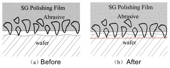
Sol-gel polishing technology is a green and efficient polishing method, through the use of semi-consolidated abrasives and flexible substrates, by virtue of the flexible characteristics of the soft matrix, the "tolerance" effect of the abrasive particles is achieved to achieve ultra-smooth and low defect density surface on the extremely hard semiconductor substrate. This method combines chemical and mechanical action to effectively polish extremely hard semiconductor substrates without causing severe surface or subsurface damage. Compared with traditional CMP, sol-gel polishing technology can significantly reduce the surface roughness in a short time and achieve a higher material removal rate. Due to its good flexibility, the soft matrix can work under lower polishing pressure, reduce the pressure demand on the workpiece and equipment, reduce the wear and fall off of the wear particle, and extend the service life of the wear particle. The precursor material (usually a metal-organic compound) is converted to sol, which forms a gel through hydrolysis and condensation reactions. In the sol-gel polishing pad, the wear particles are partially fixed in the gel matrix, which can provide a certain mechanical strength while maintaining the movement of the wear particles. Domestic scholars used this technology to process HTHP single crystal diamond (111) surface, polishing 22h, the surface roughness from 230nm to 1.3nm. By the way, the capacitance effect refers to that in the polishing process, when the abrasive touches the machined surface, due to the presence of soft matrix, the more prominent abrasive can produce rebound, thus ensuring that the surface abrasive can process the workpiece approximately in the same horizontal plane, avoiding the damage of the larger size abrasive to the machined surface, and obtaining uniform material removal. A better polishing effect is achieved.
In summary, silicon carbide, as a new star in the semiconductor material industry, is leading the innovation of microelectronics technology with its unique performance advantages. Its wide application not only promotes the technological progress in the high-end field, but also profoundly affects every link of the semiconductor industry chain. However, the high hardness properties of silicon carbide also pose challenges for its processing. In the face of this problem, researchers are actively exploring innovative solutions, such as sol-gel polishing technology, these emerging technologies not only improve processing efficiency and surface quality, but also open up new ways for the application and development of silicon carbide materials in a wider range of fields. With the continuous progress of technology, silicon carbide materials will certainly play a more important role in the future field of science and technology.