Aluminum nitride (AlN) ceramics, as a material with excellent thermal conductivity, mechanical properties and electrical properties, have been widely used in large-scale integrated circuits and electronic packages in recent years. Its excellent properties make it an ideal cooling substrate and packaging material. However, due to the high hardness, high brittleness and low fracture toughness of aluminum nitride ceramics, surface defects and sub-surface damage are easy to occur during processing. In order to meet the demand for ultra-smooth surface of integrated circuits, the polished surface of aluminum nitride substrate needs to achieve extremely high flatness and low surface roughness. This also makes how to effectively reduce the defects and damage in the processing has become an important research topic in the field of ultra-precision machining. In recent years, plasma assisted polishing (PAP) technology has gradually become an important means of polishing aluminum nitride ceramics because of its effective treatment of difficult-to-process materials.
Characteristics and processing challenges of aluminum nitride ceramics
Aluminum nitride ceramics not only have excellent thermal conductivity, but also have corrosion resistance and good electrical properties. These characteristics make it widely used in high-performance electronic components, especially in electronic device packaging where efficient heat dissipation is required. The lightweight design of aluminum nitride substrate can effectively reduce the volume of electronic devices, while reducing the internal resistance of the package, which is conducive to the heat dissipation of the chip. Aluminum nitride ceramic hardness and brittleness, however, makes it very easy to produce in the process of machining mechanical damage, causing surface micro cracks, pits, and the surface defects. These defects not only affect the mechanical strength of material, also can reduce the heat dissipation performance and electrical properties, which affect the stability of the electronic device and service life. Therefore, in the processing of aluminum nitride ceramics, how to obtain ultra-smooth surface, reduce surface roughness and reduce damage depth is always the focus of manufacturing enterprises and research institutions.
Although the traditional mechanical polishing method can achieve a certain surface flatness, it is easy to cause a lot of mechanical damage, and it is difficult to effectively meet the high precision demand of current integrated circuits. In contrast, plasma assisted polishing technology provides an effective solution for the processing of aluminum nitride substrates.
Overview of plasma assisted polishing (PAP) technology
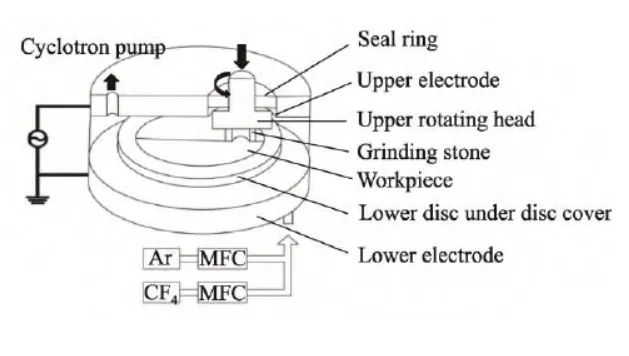
Plasma assisted polishing (PAP) is a combination of plasma modification and soft abrasive to remove dry polishing technology. The principle is to modify the surface of aluminum nitride ceramic by plasma irradiation, so that the chemical properties of the surface are changed, and then the soft abrasive is used to remove the material under the following low pressure. Compared with traditional mechanical polishing, plasma assisted polishing can effectively reduce the surface stress concentration and reduce the mechanical damage in the polishing process. The plasma in PAP technology mainly stimulates the surface of aluminum nitride ceramic to form a modified layer, which is easier to be removed by abrasive, thus greatly reducing the surface cracks and microscopic defects caused by mechanical action. In addition, the non-contact processing method of the plasma reduces the direct contact between the abrasive tool and the workpiece, reducing the friction force and further reducing the sub-surface damage.
PAP technique in the application of aluminum nitride ceramic polishing and advantages
1. Reduce surface defects: Because PAP technology changes the surface properties of materials through plasma irradiation, the removal of surface materials mainly depends on the joint action of chemical and physical effects, so it can effectively reduce micro-cracks and dents generated in the mechanical polishing process. In integrated circuit chip applications, surface roughness Ra ≤ 8 nm is a common requirement, and PAP technology can better achieve this goal while keeping the damage depth at the nanometer level. This is of great significance for improving the overall processing quality of aluminum nitride substrate.
2. Reduce subsurface damage: Traditional polishing methods often cause stress concentration inside the material during material removal, resulting in invisible subsurface damage. This damage is often difficult to detect by surface observation, but can significantly affect the mechanical and thermal properties of the material. Plasma assisted polishing technology significantly reduces the formation of sub-surface defects by reducing mechanical contact and reducing grinding forces, ensuring material integrity.
3. Improve processing accuracy: PAP technology can accurately control the energy and irradiation time of the plasma, adjust the removal rate of the material and the thickness of the surface modification layer, and thus achieve a higher precision polishing effect. For aluminum nitride ceramic substrates that require extremely high surface accuracy, PAP technology can achieve surface smoothness of RMS < 2 nm, which is particularly important for the semiconductor and electronic packaging industry.
4. Environmental protection of dry processing: PAP technology, as a dry polishing process, does not need to use a large amount of polishing liquid, reducing the chemical waste generated in the polishing process, in line with the requirements of modern manufacturing industry for environmental protection and sustainable development. In addition, the use of chemicals is reduced, which also reduces costs and environmental pollution.
Limitations and future development of PAP technology
Although plasma assisted polishing in the machining process of aluminum nitride ceramic shows many advantages, but it also has some limitations. First of all, the PAP technology compared with traditional mechanical polishing, equipment cost is higher, and the material removal rate is relatively low, limiting its application in large-scale processing. In addition, due to the small irradiation range of plasma, the processing area is limited, which to some extent limits the application of PAP in large-size substrate processing.
In the future, the research focus of PAP technology should focus on improving the material removal rate and the cost-benefit ratio of equipment. At the same time, combined with other advanced ultra-precision machining technologies, such as laser-assisted polishing or ion beam polishing, or will be an effective way to improve the efficiency and quality of aluminum nitride ceramic polishing.
Conclusion
Plasma assisted polishing technology with its significantly reduced in the aluminum nitride ceramic machining surface defect and the surface damage of advantage, gradually become one of the important technology in the field of ultra-precision machining. Although the equipment cost is high and the material removal rate is low, with the continuous progress of technology and the expansion of applications, PAP technology is expected to become one of the mainstream processing means to deal with high hardness and high brittleness materials in the future. In the field of semiconductor and electronic packaging, PAP technology has a broad application prospect and is worth further research and promotion.