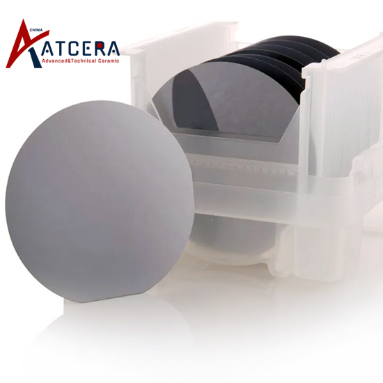
With the continuous progress of semiconductor technology, silicon carbide (SiC), as a high-performance material, has shown great application potential in the field of power electronic devices. However, in the preparation process of silicon carbide substrate, surface quality control is particularly critical, especially after thinning, grinding and polishing and other processes to obtain ultra-smooth surface. Among them, chemical mechanical polishing (CMP), as one of the key steps, is of great significance for removing the damaged layer left by the previous process and achieving high surface levelling. However, the traditional CMP process faces the problem of low material removal rate (MRR), which directly affects the production efficiency and cost. Therefore, exploring new technologies to improve the CMP efficiency of SiC substrate has become the focus of current research.

1. Basic principles and challenges of SiC substrate CMP
The surface damage depth of the thinned or ground SiC substrate is usually 2-5μm and requires further treatment by CMP.
CMP technology is based on the "chemical + mechanical" composite principle, through the combination of oxide layer formation and mechanical removal, to achieve surface smoothing.
2. Low MRR is the main problem of SiC substrate CMP, and the CMP efficiency of SiC is significantly lower than that of silicon substrate.
The impact of low MRR on production efficiency and cost:
Lower MRR results in longer time consuming SiC substrate CMP steps, increasing processing time and cost.
Even if the existing CMP method can produce qualified 4H-SiC substrate, low efficiency is still the bottleneck restricting its large-scale application.

CMP polishing process
3. Technical progress to improve CMP efficiency:
To meet the low MRR challenge, the industry has developed double-sided, batch polishing technology.
These advanced technologies have significantly reduced CMP man-hours, such as the CMP polishing time for a single batch of 10 substrates from 3-5 hours to 1 hour.
Double-sided polishing technology not only improves efficiency, but also helps maintain consistency and flatness on both sides of the substrate.
In summary, the improvement of chemical-mechanical polishing efficiency of silicon carbide substrate is the key to promote its wide application. Through the development of advanced technologies such as double-sided and batch polishing, the problem of low material removal rate in the traditional CMP process is effectively solved, the processing time is significantly shortened, and the production cost is reduced. In the future, with the continuous improvement of the performance requirements for SiC materials and the continuous innovation of polishing technology, we have reason to believe that the preparation of SiC substrates will be more efficient and economical, laying a solid foundation for the further development of power electronic devices. Therefore, the continuous exploration and optimization of CMP process will be an important way to promote the wide application of SiC materials in the semiconductor field.


