With the wide application of silicon carbide (SiC) in semiconductor devices, the quality requirements of silicon carbide substrates are becoming more and more stringent. SiC devices have strict regulations on the surface thickness change, surface roughness (Ra), machining damage and residual stress of the liner film. However, the SiC substrate after cutting and stripping often has problems such as damaged layer, high surface roughness and poor flatness. These problems must be solved by effective flattening process to obtain high quality polished sheet for subsequent epitaxy process. This article will focus on the grinding and grinding technology in the SiC substrate flattening process, and compare and analyze their advantages and disadvantages.

1. Current situation and limitation of grinding process
The grinding process has a high share of the market, including two stages of rough grinding and fine grinding, and requires single-side mechanical polishing (DMP) before chemical mechanical polishing (CMP). Its advantage is that the cost is relatively low, but there are disadvantages such as cumbersome processes, low automation level, high fragmentation risk, low flexibility and certain impact on the environment.
2. Advantages and adaptability of grinding process
The grinding process, as an alternative to the grinding process, provides higher material removal rates and better control of wafer thickness and flatness. It uses different abrasives and grinding techniques, such as diamond grinding wheels, to achieve a finer and more uniform surface treatment. The grinding process is excellent in terms of automation and flexibility, suitable for single chip processing, and can better adapt to the processing needs of large-size wafers.

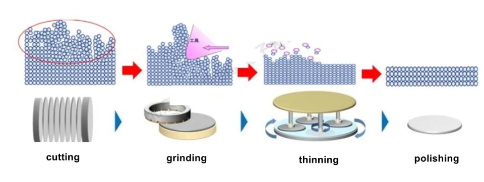
SiC substrate flattening process diagram
The grinding process usually includes two stages of coarse grinding and fine grinding, and the damaged layer of the substrate surface is gradually removed by different particle sizes of the abrasive material to improve the surface smoothness. However, the process has many problems. First of all, the process is more complicated, from rough grinding to fine grinding to DMP and CMP, requires multiple steps, increasing the processing time and cost. Secondly, the level of automation is not high, resulting in low production efficiency. For large wafers, there is a high risk of fragmentation due to mechanical stress during processing. In addition, the flexibility of the grinding process is low, which is not conducive to single chip processing, and the use of grinding fluid has a certain impact on the environment.
The grinding process uses highly efficient abrasives such as diamond wheels to achieve rapid flattening of SiC substrates with higher material removal rates. Compared with grinding process, grinding process has the following advantages: first, high degree of automation, can significantly improve production efficiency; The second is good flexibility, suitable for single piece processing, can be customized according to different needs; Third, it can better adapt to the processing needs of large-size wafers and reduce the risk of fragmentation. In addition, the grinding process enables a finer and more uniform surface finish, providing a better substrate for subsequent CMP processes.
In summary, the grinding and grinding techniques in the SiC substrate flattening process have their advantages and disadvantages. Although the grinding process cost is low, but the process is cumbersome, the level of automation is not high, the risk of fragmentation is high and the flexibility is low, which limits its further development. In contrast, the grinding process shows obvious advantages in terms of automation, flexibility, material removal rate and surface treatment quality, which is more suitable for the high-quality requirements of SiC substrates in the modern semiconductor industry. Therefore, with the continuous progress of semiconductor technology, grinding process is expected to become the mainstream technology of SiC substrate flattening. In the future, grinding process parameters should be further optimized to improve processing efficiency and quality to meet the increasingly stringent substrate requirements of SiC devices.


