In the field of semiconductor materials, silicon carbide (SiC) with its excellent thermal conductivity, wide band gap characteristics, high breakdown electric field strength and high electron mobility, is gradually becoming a research and development hotspot, leading the innovation of a new generation of electronic devices. As a substrate material for key components, the broad application prospects of silicon carbide are self-evident, from high-efficiency power electronics to high-frequency communication chips, its figure is everywhere. However, the extremely high hardness of silicon carbide materials (Mohs hardness of about 9.5) is like a double-edged sword, both giving it excellent physical properties, but also set up numerous obstacles for its processing.
Faced with the difficult problem of polishing and grinding silicon carbide substrate, traditional processing methods are often inadequate, inefficient and costly. It is in this context that the metal friction induced reaction grinding technology came into being, and opened up a new path for the efficient processing of silicon carbide. This technology cleverly uses the chemical reaction produced by metal and silicon carbide friction at high temperature, through the continuous formation and removal of the reaction metamorphic layer, to achieve high speed and low damage removal of silicon carbide materials. This innovation not only overcomes the processing problems caused by the high hardness of silicon carbide, but also significantly improves the processing efficiency and surface quality.
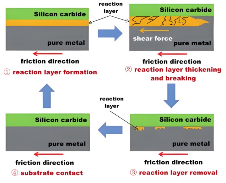
It is worth noting that the metal friction-induced reaction grinding technology needs to be applied under precisely controlled conditions to avoid the decomposition of silicon carbide at high temperatures and the formation of unstable compounds with the metal, thus exacerbating tool wear. The experimental data show that the selection of suitable metals (such as iron, pure nickel) as friction media can achieve differentiated and efficient removal of different surfaces of silicon carbide substrate (carbon and silicon). Due to its structural stability, the surface quality of carbon surface is almost free of damage. Although there are crystal defects in the silicon surface, the material removal rate can reach 534µm/h under the friction of pure nickel, showing the great potential of this technology under certain conditions.
Looking forward to the future, metal friction induced reaction grinding technology is expected to achieve a wider application in the field of silicon carbide substrate processing. With the deepening of the research and the maturity of the technology, the technology is expected to expand to the processing of large-size silicon carbide wafers, and further improve the manufacturing efficiency and yield of silicon carbide devices. At the same time, combined with other advanced processing technologies, such as ultra-precision polishing and laser-assisted processing, it is expected to achieve comprehensive optimization of silicon carbide material processing and promote the silicon carbide semiconductor industry to a new height.
In short, silicon carbide substrate processing challenges and opportunities coexist, and the emergence of metal friction induced reaction grinding technology provides an innovative solution to this problem. With the continuous progress of technology and the continuous expansion of application fields, silicon carbide semiconductor materials will certainly play a more important role in the future development of electronic science and technology.