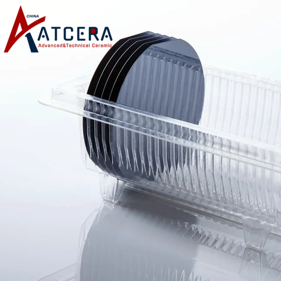
Silicon carbide substrate, as a new generation of semiconductor products, has shown great application potential in the field of power electronic devices because of its excellent physical and chemical properties. However, high efficiency and low loss cutting of SiC ingot is one of the key technologies restricting its mass production. At present, mortar wire cutting and diamond wire cutting are the two mainstream technologies in SiC ingot cutting, and they have significant differences in the ways of abrasive introduction, processing efficiency, material loss and environmental impact. This article aims to compare and analyze the characteristics of these two cutting technologies, and discuss the optimization direction of SiC cutting process.

1. Abrasive import mode and processing efficiency
· mortar wire cutting: using free abrasive, the processing speed is relatively slow.
· diamond wire cutting: through electroplating, resin bonding and other methods to fix the abrasive particles, cutting speed increased by more than 5 times, significantly improve production efficiency.
2. Material loss and film output rate
· mortar wire cutting: low output rate, large material loss.
· diamond wire cutting: the output rate is increased by 15% to 20%, the material loss is significantly reduced, and the economic benefit is improved.
3. Environmental protection advantages
· Diamond wire cutting: Less waste and wastewater production, more environmentally friendly.
4. Technical challenges and coping strategies
· Diamond wire cutting: There are challenges in crystal control and cutting loss control.
· Coping strategy: The current industry adopts the strategy of mortar wire cutting as the main and diamond wire cutting as the auxiliary, the use ratio is about 5:1. In the future, it is necessary to further optimize the diamond wire cutting technology to improve its competitiveness in SiC cutting.
5. Processing loss analysis of SiC materials
· mortar wire cutting loss:
· Notch loss: up to 150-200 microns.
· Polishing loss: Surface damage needs to be repaired by rough grinding, fine grinding and CMP processes.
· back thinning loss: The initial thickness setting is high, the back thinning is required to reduce resistance.

SiC cutting loss and damage
In summary, the diamond wire cutting technology in the cutting of SiC ingot shows significant processing speed advantages, lower material loss and environmental protection advantages, but its crystal control and cutting loss control still need to be further optimized. At present, the complementary use strategy of mortar wire cutting and diamond wire cutting is a common practice in the industry. In the future, with the continuous progress of diamond wire cutting technology and the reduction of costs, it is expected to occupy a dominant position in the SiC cutting field. At the same time, in view of the loss problem in the processing of SiC materials, it is necessary to further explore more efficient and low-loss cutting and polishing processes to promote the efficient and low-cost production of SiC semiconductor materials and promote its wide application in the field of power electronic devices.


