Although the processing of silicon carbide substrate is difficult, in order to make the application of single crystal silicon carbide in electronic components become the future direction of development, so that silicon carbide devices are large-scale application and promotion, it is necessary to find a way to solve the problem of difficult silicon carbide processing.
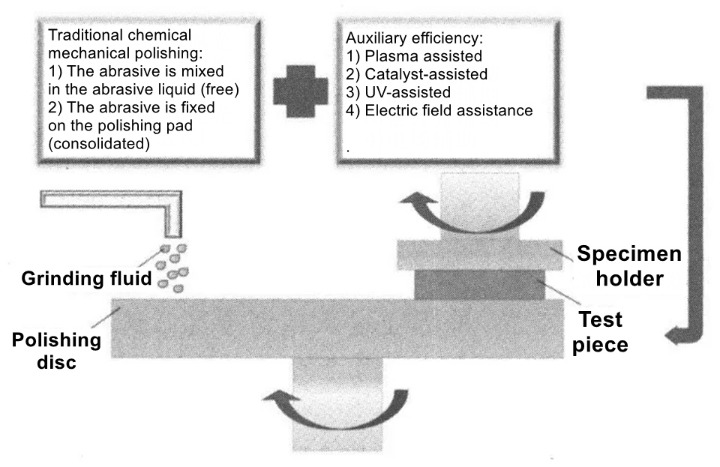
At present, the SiC material processing technology mainly has the following processes: directional cutting, chip rough grinding, fine grinding, mechanical polishing and chemical mechanical polishing (fine polishing). Among them, chemical-mechanical polishing is the final process, and its process method selection, process route arrangement and process parameter optimization directly affect the polishing efficiency and processing cost.
However, due to the high hardness and chemical stability of SiC materials, the material removal rate in the traditional CMP polishing process is low. Therefore, the industry began to study the auxiliary efficiency technology supporting the flattening ultra-precision machining technology, including plasma assisted, catalyst assisted, ultraviolet assisted and electric field assisted, as follows:
01 Plasma assisted technology
YAMAMURA Kazuy et al. first proposed the plasma-assisted polishing (PAP) process, which is an auxiliary chemical-mechanical polishing that oxidizes surface materials to a softer oxide layer through plasma, while still removing materials by abrasive friction and wear.
The basic principle is: through the RF generator reaction gas (such as water vapor, O, etc.) to produce a plasma containing free groups (such as OH free groups, O free radicals), with strong oxidation capacity of free groups on the surface of the SiC material oxidation modification. A soft oxide layer is obtained, and then the oxide layer is removed by polishing with soft abrasives (such as CeO2, Al2O3, etc.), so that the surface of SiC material reaches the atomic level smooth surface. However, due to the high price of PAP process test equipment and processing costs, the promotion of PAP process processing SiC chips is also limited.
02 Catalyst assisted process
In the industrial field, in order to explore the high-efficiency ultra-precision machining technology of SiC crystal materials, researchers use reagents for catalytic assisted chemical-mechanical polishing. The basic mechanism of material removal is that the soft oxide layer is formed on the SiC surface under the catalysis of reagents, and the oxide layer is removed by the mechanical removal of abrasive. For a high quality surface. In the literature, Fe3O4 catalyst and H2O2 oxidizer were used to assist the enhancement of chemical mechanical polishing technology with diamond W0.5 as abrasive. After optimization, the surface roughness Ra=2.0 ~ 2.5 nm was obtained at the polishing rate of 12.0 mg/h.
03 UV-assisted technology
In order to improve the SiC surface flattening processing technology. Some researchers have used ultraviolet radiation to assist catalysis in chemical-mechanical polishing process. Uv photocatalytic reaction is one of the strong oxidation reactions. Its basic principle is to produce active free radicals (·OH) by photocatalytic reaction between photocatalyst and electron catcher under the action of UV light.
Due to the strong oxidation of OH free groups. The oxidation reaction occurs on the SiC surface layer to generate a softer SiO2 oxide layer (MOE hardness is 7), and the softened SiO2 oxide layer is easier to be removed by abrasive polishing; On the other hand, the bonding strength between the oxide layer and the surface of the wafer is lower than the internal bonding strength of the SiC wafer, which reduces the cutting force of the abrasive in the polishing process, reduces the scratch depth left on the surface of the wafer, and improves the surface processing quality.
04 Electric field assisted technology
In order to improve the removal rate of SiC materials, some researchers have proposed electrochemical mechanical polishing (ECMP) technology. The basic principle is: by applying direct current electric field to the polishing liquid in the traditional chemical mechanical polishing treatment, the oxidation layer is formed on the SiC polishing surface under electrochemical oxidation, and the hardness of the oxide layer is significantly reduced. Abrasive is used to remove the softened oxide layer to achieve efficient ultra-precision machining. However, it should be noted that if the anode current is weak, the machining surface quality is better, but the material removal rate does not change much; If the anode current is strong, the material removal rate is significantly increased. However, too strong anode current will lead to lower surface accuracy and porosity.
In short, chemical-mechanical polishing is still the most potential flattening ultra-precision machining method for SiC materials, but in order to obtain high-quality SiC wafers more efficiently, the above mentioned auxiliary processes are potential options. However, due to the lack of relevant studies, the impact on SiC materials is still lack of predictability. Therefore, if we can deeply study the influence of related auxiliary processes on chemical-mechanical polishing technology, and further reveal the processing mechanism of chemical-mechanical polishing auxiliary efficiency enhancement technology by quantitative and qualitative research means, it will be of great significance for realizing the industrialization application and promotion of SiC materials.