ITO ceramic sputtering target

Indium Tin Oxide Sputtering Target ITO Ceramic Target

ITO sputtering target is a composite material composed of indium oxide (In2O3) and tin oxide (SnO2), of which indium oxide as the main component, provides the basic electrical and optical properties of the material, by adjusting the proportion of SnO2 to optimize its conductivity and transparency, also to improve its chemical stability and wear resistance, good electrical and thermal conductivity and high strength. It is used to manufacture various displays, such as flat panel display (PFD), liquid crystal displays (LCD), organic electroluminesence display(OELD), electroluminescence display (EL), field emission display (FED), plasma displays (PDP), etc., and can also be used to manufacture solar cell films and glass with special functions, such as conductive glass, thermal insulation glass, anti-ultraviolet glass, anti-fog glass, etc.

  • Brand:

    ATCERA
  • Item NO.:

    AT-JS-ITO1001
  • Materials

    ITO
  • Shapes

    Plate
  • Applications

    Semiconductor , Electronics and Electricity , Photovoltaic Cell Industry
ITO Sputtering Target

Advantages of Indium Tin Oxide Sputtering Target


ITO sputtering target has high sintering density, uniform microstructure, good electrical and thermal conductivity, high strength, also with properties to reduce nodulation phenomenon and the appearance of micro arc.


application of Indium tin oxid sputtering target

Applications of ITO Ceramic Sputtering Target


ITO sputtering target is used to manufacture various displays, such as flat panel display (PFD), liquid crystal displays (LCD), organic electroluminesence display(OELD), electroluminescence display (EL), field emission display (FED), plasma displays (PDP), etc., and can also be used to manufacture solar cell films and glass with special functions, such as conductive glass, thermal insulation glass, anti-ultraviolet glass, anti-fog glass, etc.


Size Chart of Indium Tin Oxide Sputtering Target


Committed to providing optimal indium tin oxid sputtering target customized to your precise needs. Our devoted team guarantees careful adherence to your instructions, aiming to surpass customer expectations. Moreover, we provide the flexibility of customized sizes to meet your unique requirements.


Please provide dimension and weight proportion of In2O3 to SnO2 for customization.


ITO Sputtering Target
Item NO. Specifications In2O3:SnO2 Notes
AT-JS-ITO1001 Ф25.4*3.175mm 90:10wt% Round
AT-JS-ITO1002 Ф25.4*6.35mm 90:10wt% Round
AT-JS-ITO1003 Ф50.8*3.175mm 90:10wt% Round
AT-JS-ITO1004 Ф50.8*6.35mm 90:10wt% Round
AT-JS-ITO1005 Ф76.2*3.175mm 90:10wt% Round
AT-JS-ITO1006 Ф76.2*6.35mm 90:10wt% Round
AT-JS-ITO1007 Ф101.6*3.175mm 90:10wt% Round
AT-JS-ITO1008 Ф101.6*6.35mm 90:10wt% Round
AT-JS-ITO1009 Ф12-500mm*T:0.1-15mm Customized Round
AT-JS-ITO2001 Ф50-185mm*L:350-2200mm Customized Rotating
AT-JS-ITO3001 L:20*500*W:10-2200*T:1-25mm Customized Flat


Technical Data

  Indium tin oxide sputtering target Alumina sputtering target
Purity 99.99% 99.99%


Valuable Information


indium tin oxid sputtering target

Indium Tin Oxide Sputtering Targets Packing


Indium tin oxide ceramic sputtering targets are carefully packaged in appropriate containers to avoid any potential damage.


Customization Advantages


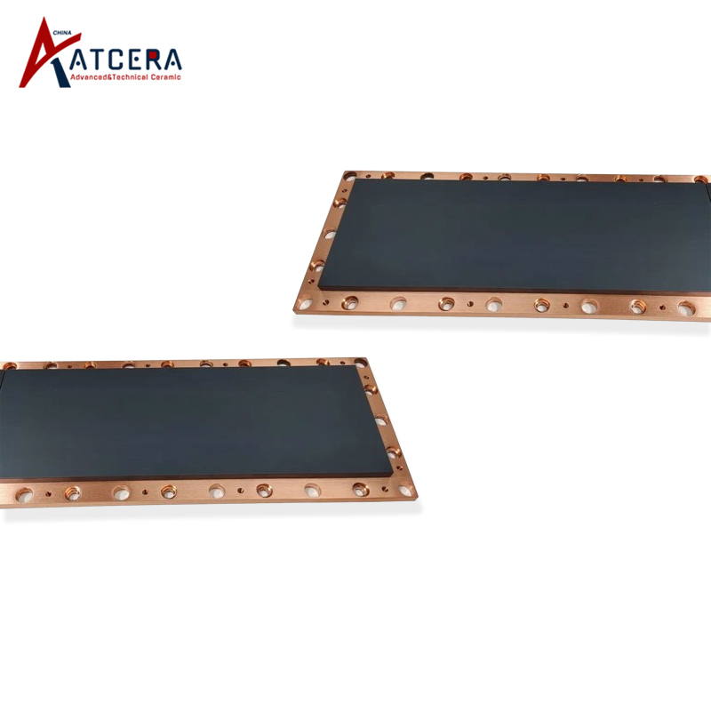
1. According to your application scenario, analyze the needs, choose the appropriate material and processing plan.


2. Professional team, quick response, can provide solutions and quotations within 24 hours after confirming the demand.


3. Flexible business cooperation mechanism, support at least one piece of quantity customization.


4. Quickly provide samples and test reports to confirm that the product meets your needs.


5. Provide product use and maintenance suggestions to reduce your cost of use.

Related Blog
Silicon Carbide Substrate Processing Challenges with Innovative Applications Of Metal Friction-induced Reaction Grinding Technology
In the field of semiconductor materials, silicon carbide (SiC) with its excellent thermal conductivity, wide band gap characteristics, high breakdown electric field strength and high electron mobility, is gradually becoming a research and development hotspot, leading the innovation of a new generation of electronic devices. As a substrate material for key components, the broad application prospect...
Exploration Of Laser Processing Technology Of AlN Substrate To Realize High Quality Flat Machining Surface
With the rapid development of electronic technology, the integration and performance requirements of large-scale integrated circuits are increasing day by day. As a key supporting material, aluminum nitride ceramics have become an ideal cooling substrate and packaging material because of their excellent thermal conductivity, mechanical strength, corrosion resistance and excellent electrical proper...
ELID Grinding Process Of AlN Substrate: Solving The Difficult Problem Of Machining High-hardness Brittleness
With the rapid development of microelectronics technology, the requirements for electronic packaging materials are increasingly stringent. Aluminum nitride ceramics, with its excellent thermal conductivity, excellent mechanical properties, corrosion resistance and excellent electrical properties, become the leader of large-scale integrated circuit cooling substrate and packaging materials. However...
AlN Ceramic Magnetorheological Polishing Process Achieves High-Quality Surface For AlN Substrate
Today, with the rapid development of the electronics industry, aluminum nitride ceramics have become the first choice for large-scale integrated circuit cooling substrates and packaging materials because of their excellent thermal conductivity, excellent mechanical properties, corrosion resistance and good electrical properties. Especially in the pursuit of miniaturization and high performance int...
Chemical Mechanical Polishing Of AlN Substrate: The Key Path To Overcome Micro-cracks And Subsurface Damage
In the field of microelectronic packaging, aluminum nitride ceramics are gradually becoming the preferred material for high-performance chip cooling substrates due to their excellent thermal conductivity, mechanical strength and electrical properties. However, its high hardness and high brittleness can easily cause surface micro-cracks and sub-surface damage during processing, which directly affec...
Study On Thermal Conductivity Of Aluminum Nitride Substrate And Analysis Of Influence Of Oxygen Impurity
For a long time, most of the substrate materials of high-power hybrid integrated circuits have been using Al2O3 and BeO ceramics, but the thermal conductivity of the Al2O3 substrate is low, and the thermal expansion coefficient is not well matched with Si. Although the comprehensive performance of BeO is excellent, its high production cost and highly toxic shortcomings limit its application and pr...
Evolution Of Ceramic Substrate Materials: Breakthroughs From Alumina To Aluminum Nitride And Silicon Nitride
In today's rapidly changing electronics industry, ceramic substrate materials as a key basis for supporting high-performance electronic devices, its performance and characteristics directly affect the overall performance and reliability of electronic products. From the early alumina ceramics to the later aluminum nitride, silicon nitride and other new materials, the development of ceramic substrat...
The Applicability of Aluminum Nitride Substrate as a Packaging Material for Enhancing Heat Dissipation in Power Devices
With the rapid development of electronic technology, the comprehensive performance of electronic chips is improving day by day, but the overall size is shrinking. This trend brings significant performance improvements, but it also comes with a serious challenge - a dramatic increase in heat flux. For electronic devices, even a small increase in temperature can have a significant impact on their pe...
Thermal Conductivity Improvement of Silicon Nitride Substrate
In the field of advanced ceramic materials, silicon nitride (Si3N4) has attracted much attention for its excellent mechanical strength, chemical stability and high temperature properties. However, the thermal conductivity of silicon nitride ceramics, as one of the key factors affecting its wide application, has been an important subject in materials science research. This paper aims to investigate...
Exploring Lattice Vibration Mechanism And Sintering Assistant Strategy Of Silicon Nitride Substrates
In cutting-edge technologies such as high-performance electronic packaging, aerospace and energy conversion, silicon nitride (Si3N4) substrate materials are highly regarded for their excellent mechanical properties, chemical stability and high temperature resistance. However, the thermal conductivity of silicon nitride, as one of the key factors affecting its wide application, has always been...

Related Products

FAQ

Although our primary focus is on advanced ceramic materials such as alumina, zirconia, silicon carbide, silicon nitride, aluminum nitride, and quartz ceramics, we are always exploring new materials and technologies. If you have a specific material requirement, please contact us, and we will do our best to fulfill your needs or find suitable partners.

Absolutely. Our technical team possesses profound knowledge of ceramic materials and extensive experience in product design. We are happy to provide you with material selection advice and product design support to ensure optimal performance for your products.

We do not have a fixed minimum order value requirement. We always focus on meeting our customers' needs, and we strive to provide quality service and products regardless of the order size.

In addition to ceramic products, we also provide a range of additional services, including but not limited to: customized ceramic processing services based on your needs, using blanks or semi-finished blanks produced by yourself; if you are interested in outsourced ceramic packaging and metallization services, please contact us for further discussion. We are always committed to providing you with a one-stop solution to meet your various needs.

Yes, we do. No matter where you are located globally, we can ensure the safe and timely delivery of your order.

Send Your inquiry

Upload
* File ONLY PDF/JPG./PNG. Available.
Submit Now

Contact With Us

Contact With Us
Simply fill out the form below as best you can. And don't sweat the details.
Submit
Looking for Video?
Contact Us #
19311583352

Office Hours

  • Monday to Friday: 9:00 AM - 12:00 PM, 2:00 PM - 5:30 PM

Please note that our office hours are based on Beijing Time, which is eight hours ahead of Greenwich Mean Time (GMT). We appreciate your understanding and cooperation in scheduling your inquiries and meetings accordingly. For any urgent matters or queries outside our regular hours, feel free to contact us via email, and we will get back to you as soon as possible. Thank you for your business, and we look forward to serving you.

Home

Products

whatsApp

contact