Beryllium oxide substrate

Beryllium Oxide Ceramic Substrate BeO Substrate

Beryllium oxide ceramic substrate is made of beryllium oxide powder as raw material and sintered at high temperature after forming. It has excellent thermal conductivity, low dielectric constant and dielectric loss, reliable insulation performance, high temperature resistance and corrosion resistance. It is widely used in microwave devices, communication devices, high brightness LED, power electronic devices, especially various high-power devices and integrated circuits. The high thermal conductivity of beryllium oxide ceramic substrates can provide a strong guarantee for their stable operation.

  • Brand:

    ATCERA
  • Item NO.:

    AT-BeO-J1001
  • Materials

    BeO
  • Shapes

    Substrate
  • Applications

    Semiconductor , Electronics and Electricity
Beryllium oxide ceramic substrate

Properties of Beryllium Oxide Ceramic Substrate


1. With excellent thermal conductivity, up to 310W/(℃*m), which is around 10 times of alumina substrate. It has high temperature resistance and thermal shock resistance is good.


2. Good electric insulation, high breakdown voltage, large current carrying capacity.


3. Low dielectric constant, which is around 7, and the dielectric loss is very low, which can reduce the energy loss during signal transmission.

Beryllium oxide substrate

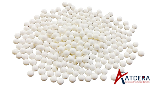
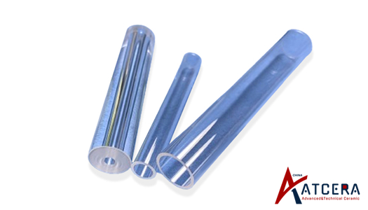
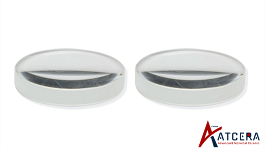
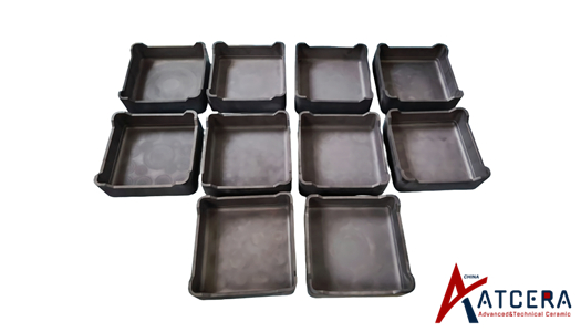
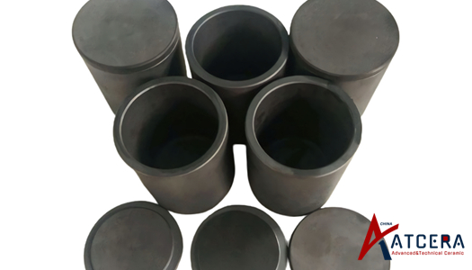
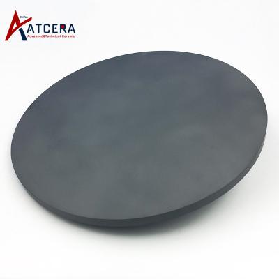
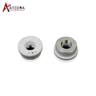
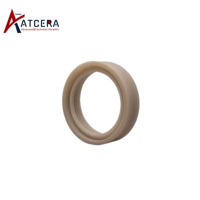
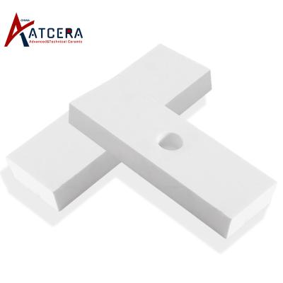
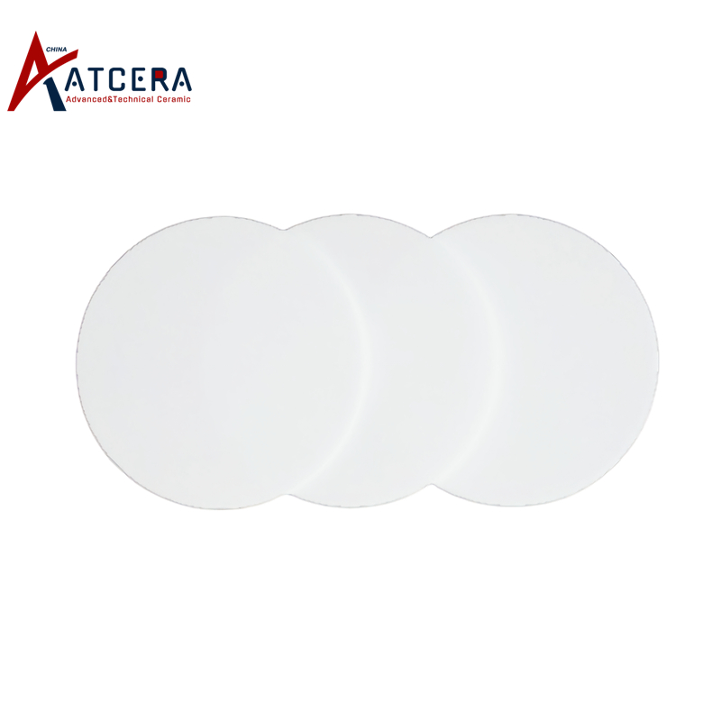
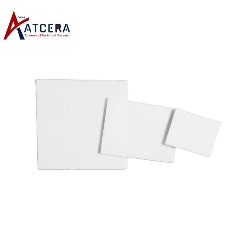
Applications of BeO Substrate


Beryllium oxide ceramic substrate has excellent thermal conductivity performance, it is mainly used in semiconductor, electronics and other microelectronics device manufacturing, as the substrate of chips and electronic components, including integrated circuit (IC), radio frequency (RF) devices, piezoelectric components, photoelectric components, sensors, MEMS and other micro electronic devices. As a high-performance material, beryllium oxide ceramic substrate can provide a stable support platform to ensure normal operation and performance of the components.


1. LED chip: beryllium oxide ceramic substrate has excellent thermal conductivity and mechanical strength, can be used to manufacture high-brightness LED chip, greatly improve the luminous efficiency of LED.


2. Electronic components: beryllium oxide ceramic substrate can be used to manufacture a variety of high-power and high-performance electronic components, such as power semiconductor devices, microwave devices, sensors, radio frequency modules, etc., to achieve more stable working conditions and higher performance indicators.


3. Photoelectric devices: beryllium oxide ceramic substrate can be used in the manufacture of optoelectronic parts, including laser diodes, solar cells, photodetectors, optical communication devices, etc.


Size Chart for Beryllium Oxide Ceramic Substrate

We are committed to delivering prime beryllium oxide substrates tailored to your exact specifications. Our dedicated team ensures meticulous adherence to your instructions, striving to exceed customer expectations. Additionally, we offer the flexibility of customized sizes to accommodate your unique requirements.


Drawings and parameter requirements shall be provided if customized design request.


Machining Tolerance: surface roughness: Ra0.05-Ra0.8; warping degree: ≤2‰.


Beryllium Oxide Ceramic Substrate Square
Item NO. L × W
(mm)
Thickness
(mm)
AT-BeO-J1001 50.8*50.8 0.38
AT-BeO-J1002 76.2*76.2 0.38
AT-BeO-J1003 101.6*101.6 0.38
AT-BeO-J1004 114.3*114.3 0.38
AT-BeO-J1005 32.1*9 0.5
AT-BeO-J1006 40*9 0.5
AT-BeO-J1007 45*2.5 0.5
AT-BeO-J1008 50.8*50.8 0.5
AT-BeO-J1009 76.2*76.2 0.5
AT-BeO-J1010 101.6*101.6 0.5
AT-BeO-J1011 114.3*114.3 0.5
AT-BeO-J1012 7*6 0.635
AT-BeO-J1013 40*30 0.635
AT-BeO-J1014 42*42 0.635
AT-BeO-J1015 50.8*50.8 0.635
AT-BeO-J1016 76.2*76.2 0.635
AT-BeO-J1017 101.6*101.6 0.635
AT-BeO-J1018 114.3*114.3 0.635
AT-BeO-J1019 25.5*19.5 1
AT-BeO-J1020 27*18.2 1
AT-BeO-J1021 36.7*9.7 1
AT-BeO-J1022 46.8*22.4 1
AT-BeO-J1023 50.8*50.8 1
AT-BeO-J1024 76.2*76.2 1
AT-BeO-J1025 101.6*101.6 1
AT-BeO-J1026 114.3*114.3 1
AT-BeO-J1027 12.7*10 1.5
AT-BeO-J1028 30*30 1.5
AT-BeO-J1029 50.8*50.8 1.5
AT-BeO-J1030 76.2*76.2 1.5
AT-BeO-J1031 101.6*101.6 1.5
AT-BeO-J1032 114.3*114.3 1.5


Beryllium Oxide Ceramic Substrate Round
Item NO. Diameter
(mm)
Thickness
(mm)
AT-BeO-J2001 20 1.0 
AT-BeO-J2002 26 1.0 
AT-BeO-J2003 30 1.0 
AT-BeO-J2004 35 1.0 
AT-BeO-J2005 50 1.0 
AT-BeO-J2006 52 1.0 
AT-BeO-J2007 60 1.0 
AT-BeO-J2008 75 1.0 
AT-BeO-J2009 100 1.0 
AT-BeO-J2010 110 1.0 
AT-BeO-J2011 20 1.2 
AT-BeO-J2012 26 1.2 
AT-BeO-J2013 30 1.2 
AT-BeO-J2014 35 1.2 
AT-BeO-J2015 50 1.2 
AT-BeO-J2016 52 1.2 
AT-BeO-J2017 60 1.2 
AT-BeO-J2018 75 1.2 
AT-BeO-J2019 100 1.2 
AT-BeO-J2020 110 1.2 
AT-BeO-J2021 20 1.5 
AT-BeO-J2022 26 1.5 
AT-BeO-J2023 30 1.5 
AT-BeO-J2024 35 1.5 
AT-BeO-J2025 50 1.5 
AT-BeO-J2026 52 1.5 
AT-BeO-J2027 60 1.5 
AT-BeO-J2028 75 1.5 
AT-BeO-J2029 100 1.5 
AT-BeO-J2030 110 1.5 
AT-BeO-J2031 20 2.0 
AT-BeO-J2032 26 2.0 
AT-BeO-J2033 30 2.0 
AT-BeO-J2034 35 2.0 
AT-BeO-J2035 50 2.0 
AT-BeO-J2036 52 2.0 
AT-BeO-J2037 60 2.0 
AT-BeO-J2038 75 2.0 
AT-BeO-J2039 100 2.0 
AT-BeO-J2040 110 2.0 
AT-BeO-J2041 20 2.5 
AT-BeO-J2042 26 2.5 
AT-BeO-J2043 30 2.5 
AT-BeO-J2044 35 2.5 
AT-BeO-J2045 50 2.5 
AT-BeO-J2046 52 2.5 
AT-BeO-J2047 60 2.5 
AT-BeO-J2048 75 2.5 
AT-BeO-J2049 100 2.5 
AT-BeO-J2050 110 2.5 
AT-BeO-J2051 20 3.0 
AT-BeO-J2052 26 3.0 
AT-BeO-J2053 30 3.0 
AT-BeO-J2054 35 3.0 
AT-BeO-J2055 50 3.0 
AT-BeO-J2056 52 3.0 
AT-BeO-J2057 60 3.0 
AT-BeO-J2058 75 3.0 
AT-BeO-J2059 100 3.0 
AT-BeO-J2060 110 3.0 


Technical Data of Beryllium Oxide Materials

BeO Type Be-97 Be-99
BeO purity ≧97% ≧99%
Density (g/cm3) ≧2.85 ≧2.85
Flexture strength (MPa) 170 190
Hardness (Hv) 1200 1250
Fracture toughness (MPa*m1/2) 2.5~3.5 2.5~3.5
Maximum working temperature (℃) 1600 1650
Thermal conductivity (W/m*K) 220-240 260-310
Thermal expansion coefficient (/℃) 7~8.5*10-6 7~8.5*10-6
Dielectric Constant (at 1MHz) 6.5 7
Breakdown Voltage (kV/mm) 15 20


*This chart illustrates the standard characteristics of the beryllium oxide materials commonly employed in the manufacturing of our BeO products and parts. Please be aware that the attributes of customized beryllium oxide products and parts may vary depending on the specific processes involved.


Usage Instructions


1. Collision and impact during use shall be to avoid damage.


2. Working temperature of beryllium oxide ceramic substrate shall be strictly controlled, long time over temperature working shall be avoided.


3. Beryllium oxide ceramic substrate has good corrosion resistance to acid, alkali, salt and other chemicals, but contact with strong acid, especially hydrofluoric acid shall be avoided.


4. The surface of beryllium oxide ceramic substrate is easy to be contaminated with dust and dirt, which may affect its performance and service life, therefore it shall be regularly cleaned during use to keep its surface clean and shiny.
 

Valuable Information


BeO Substrate Packing

BeO Substrate Packing


Beryllium oxide substrates are carefully packaged in appropriate containers to avoid any potential damage.


Customization Advantages


1. According to your application scenario, analyze the needs, choose the appropriate material and processing plan.


2. Professional team, quick response, can provide solutions and quotations within 24 hours after confirming the demand.


3. Flexible business cooperation mechanism, support at least one piece of quantity customization.


4. Quickly provide samples and test reports to confirm that the product meets your needs.


5. Provide product use and maintenance suggestions to reduce your cost of use.

Related Blog
Preparation Of Aluminum Nitride Substrate And Selection Of Sintering Additives
In the field of high-tech materials, aluminum nitride (AlN) ceramics, with its excellent thermal conductivity, excellent electrical insulation properties and excellent mechanical strength, have become the core material in key fields such as electronic packaging, power electronics and microwave communication equipment. However, the preparation of aluminum nitride substrate is a complex process...
Application Requirements Of Aluminum Nitride Substrate
Aluminum nitride (AlN) as an advanced ceramic material, because of its unique physical and chemical properties, has shown great application potential in electronic packaging, power electronics, high frequency communication and other fields. As a core component in these fields, aluminum nitride substrates not only have to meet the basic physical performance requirements, but also need to ...
Effect Of Bulk Density Of Granulated Powder On Sintering Densification Of Silicon Nitride Balls
  Si3N4 powder is the main raw material for the preparation of silicon nitride balls. Selecting the appropriate treatment method to obtain the powder with regular shape and uniform particle size distribution is the basis for the stable implementation of Si3N4 ceramic ball forming, sintering, processing and other processes. According to the different atomization methods, the spray gr...
Optimizing The Spray Granulation Process To Improve The Performance Of Si3N4 balls
Silicon nitride (Si3N4) balls show great potential in the field of high-speed, high-precision, long-life bearings due to their excellent properties, such as lightweight, self-lubricating, high insulation, non-magnetic, high elastic modulus and excellent corrosion resistance. This paper aims to discuss the optimization of the spray granulation process of Si3N4 powder, especially the press...
Silicon Nitride Ball: A New Choice For High-Tech Powder Grinding Media
With the rapid development of high-tech industry, the requirements for fineness, purity and consistency of powder materials are increasing. As a key component in the powder preparation process, the performance of grinding medium directly determines the quality of the final product. Traditionally, zirconia ceramic balls are widely used in the field of ultra-fine grinding because of their high bendi...
Application Performance And Advantage Analysis Of Silicon Nitride Ball In Ultrafine Grinding Field
With the rapid development of nanotechnology and ultrafine material science, the demand for high-purity and ultrafine powder is increasing day by day. Silicon nitride ball, with its excellent hardness, very low wear rate and good chemical stability, has gradually become the key grinding medium in the field of ultrafine grinding. The purpose of this paper is to systematically describe the performan...
Study On Performance Characteristics And Application Of Silicon Nitride Ball In Mechanical Engineering Field
With the rapid development of modern mechanical engineering technology, the requirements for material properties are increasingly stringent, especially under extreme conditions such as high temperature, high speed, strong corrosion, etc., traditional metal materials and polymer materials have been difficult to meet the needs. Silicon nitride (Si ₄) As an advanced ceramic material with excellent ov...
Sol-gel Polishing Technology: Challenges And Opportunities To Innovate Silicon Carbide Substrate Polishing
Silicon carbide, the emerging star of the semiconductor material industry, is gradually leading the innovation trend of microelectronics technology with its excellent performance indicators. Its unique thermal conductivity, far superior to traditional semiconductor materials, provides the possibility for efficient heat dissipation, especially in high-power electronic devices show unparalleled adva...
Application And Advantages Of Plasma Assisted Polishing In AlN Substrate Processing
Aluminum nitride (AlN) ceramics, as a material with excellent thermal conductivity, mechanical properties and electrical properties, have been widely used in large-scale integrated circuits and electronic packages in recent years. Its excellent properties make it an ideal cooling substrate and packaging material. However, due to the high hardness, high brittleness and low fracture toughness of alu...
Silicon Carbide Substrate Processing Challenges with Innovative Applications Of Metal Friction-induced Reaction Grinding Technology
In the field of semiconductor materials, silicon carbide (SiC) with its excellent thermal conductivity, wide band gap characteristics, high breakdown electric field strength and high electron mobility, is gradually becoming a research and development hotspot, leading the innovation of a new generation of electronic devices. As a substrate material for key components, the broad application prospect...

Related Products

FAQ

Although our primary focus is on advanced ceramic materials such as alumina, zirconia, silicon carbide, silicon nitride, aluminum nitride, and quartz ceramics, we are always exploring new materials and technologies. If you have a specific material requirement, please contact us, and we will do our best to fulfill your needs or find suitable partners.

Absolutely. Our technical team possesses profound knowledge of ceramic materials and extensive experience in product design. We are happy to provide you with material selection advice and product design support to ensure optimal performance for your products.

We do not have a fixed minimum order value requirement. We always focus on meeting our customers' needs, and we strive to provide quality service and products regardless of the order size.

In addition to ceramic products, we also provide a range of additional services, including but not limited to: customized ceramic processing services based on your needs, using blanks or semi-finished blanks produced by yourself; if you are interested in outsourced ceramic packaging and metallization services, please contact us for further discussion. We are always committed to providing you with a one-stop solution to meet your various needs.

Yes, we do. No matter where you are located globally, we can ensure the safe and timely delivery of your order.

Send Your inquiry

Upload
* File ONLY PDF/JPG./PNG. Available.
Submit Now

Contact With Us

Contact With Us
Simply fill out the form below as best you can. And don't sweat the details.
Submit
Looking for Video?
Contact Us #
19311583352

Office Hours

  • Monday to Friday: 9:00 AM - 12:00 PM, 2:00 PM - 5:30 PM

Please note that our office hours are based on Beijing Time, which is eight hours ahead of Greenwich Mean Time (GMT). We appreciate your understanding and cooperation in scheduling your inquiries and meetings accordingly. For any urgent matters or queries outside our regular hours, feel free to contact us via email, and we will get back to you as soon as possible. Thank you for your business, and we look forward to serving you.

Home

Products

whatsApp

contact