Silicon carbide ceramic wafer

Silicon Carbide Wafer SiC wafer

Silicon carbide wafer a new generation of semiconductor materials, can be used to manufacture a variety of electronic devices, such as metal oxide semiconductor field effect transistor (MOSFET), Schottky diode, photodiode, etc.

  • Brand:

    ATCERA
  • Item NO.:

    AT-SIC-JP001N
  • Materials

    SiC
  • Shapes

    Substrate
  • Applications

    Semiconductor
Silicon carbide ceramic wafer

Properties of Silicon Carbide Wafer


Silicon carbide based electronic component has good heat dissipation, high electrical conductivity, high breakdown electric field strength, large energy gap, good corrosion resistance, can meet the requirements of high power, low loss and high frequency components, and can maintain long-term stable performance in harsh environments.


1. Low energy loss: the switching loss and on-off loss of silicon carbide module are significantly lower than that of conventional IGBT module, and with the increase of switching frequency, the greater the loss difference with IGBT module;


2. Small package size: silicon carbide electronic components size is smaller than the same specification silicon based components, and has less energy loss, so it can provide higher current density;


3. High-frequency switching: electronic saturation drift rate of silicon carbide material is twice as that of silicon, which helps to improve the operating frequency of components;


4. High temperature resistance, good heat dissipation: silicon carbide band gap width and thermal conductivity is about 3 times as that of silicon, so it can withstand higher temperature, the generated heat is easier to release, which favors miniaturization and lightweight of the system.

Applications of SiC wafer

Applications of SiC wafer


Silicon carbide components can better meet the needs of high temperature, high voltage, high frequency and large power, and it is widely used in electric vehicles, photovoltaic power generation, rail transit, data centers, charging piles and other products and equipment.


1. High-power devices (conductive type): silicon carbide component has high thermal conductivity, high breakdown electric field strength, low energy loss, suitable for the production of high-power devices, such as power modules, drive modules, etc.


2. Radio frequency electronic devices (semi-insulated type): silicon carbide component has high conductivity, can meet the needs of high-frequency work, suitable for RF power amplifiers, microwave devices and high-frequency switches;


3. Photoelectronic devices (semi-insulated type): silicon carbide component has a wide energy gap and high thermal stability, suitable for production of photodiodes, solar cells and laser diodes and other devices;


4. Temperature sensor (conductive type): silicon carbide component has high thermal conductivity and thermal stability, suitable for production of wide working range and high-precision temperature sensor.


Size Chart for Silicon Carbide Wafer

We are committed to delivering optimal silicon carbide wafer tailored to your exact specifications. Our dedicated team ensures meticulous adherence to your instructions, striving to exceed customer expectations. Additionally, we offer the flexibility of customized sizes to accommodate your unique requirements.


Size,material parameter,and  processing requirements shall be provided if customized design request.


Machining Tolerance:
1. Diameter: ±0.25mm
2. Thickness: ±25μm
3. Crystal orientation: <001> ±0.5°
4. Crystal face orientation: ±0.5°
5. Edge orientation: ≤2°
Other parameter please contact ATCERA.


Drawing of Silicon Carbide Wafer Conductive

Silicon Carbide Wafer Conductive
Item NO. Diameter
(inch)
Thickness
(mm)
AT-SIC-JP001N 2 0.35
AT-SIC-JP002N 3 0.35
AT-SIC-JP003N 4 0.35
AT-SIC-JP004N 6 0.35
AT-SIC-JP005N 2 0.5
AT-SIC-JP006N 3 0.5
AT-SIC-JP007N 4 0.5
AT-SIC-JP008N 6 0.5

Drawing of SiC Substrate Round

SiC Substrate Round
Item NO. Diameter
(inch)
Thickness
(mm)
AT-SIC-CD101 2 2
AT-SIC-CD102 3 3
AT-SIC-CD103 4 4
AT-SIC-CD104 6 2
AT-SIC-CD105 8 3

Technical Data of Silicon Carbide Materials


Item Unit Index Data
Reaction-sintered SiC
(SiSiC)
Silicon Nitride Bonded With SiC
(NBSiC)
Sintered SiCn Without Pressure
(SSiC)
SiC Content % 85 80 99
Free  Silicon Content % 15 0 0
Max. Service Temp. 1380 1550 1600
Density g/cm3 3.02 2.72 3.1
Porosity % 0 12 0
Bending Strength 20℃ Mpa 250 160 380
1200℃ Mpa 280 180 400
Modulus of Elasticity 20℃ Gpa 330 220 420
1200℃ Gpa 300 / /
Thermal Conductivity 1200℃ W/m.k 45 15 74
Coefficient of Thermal Expansion K-1×10⁻⁶ 4.5 5 4.1
Vickers Hardness HV kg/mm2 2500 2500 2800


*This chart illustrates the standard characteristics of the silicon carbide materials commonly employed in the manufacturing of our SiC products and parts. Please be aware that the attributes of customized silicon carbide products and parts may vary depending on the specific processes involved.


Clean Methods


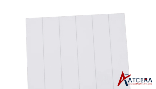
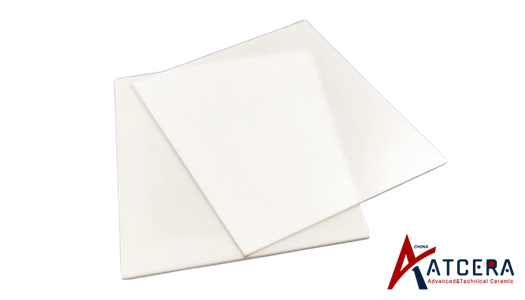
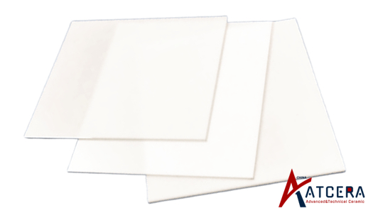
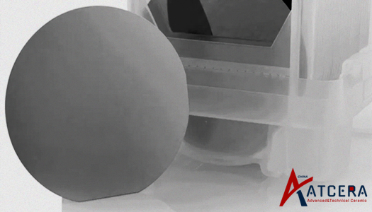
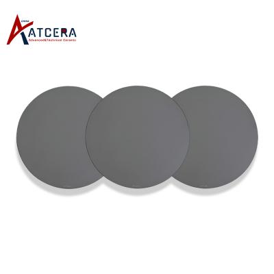
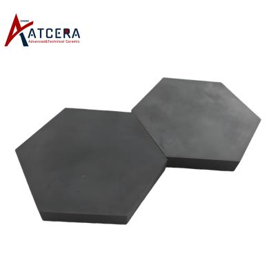
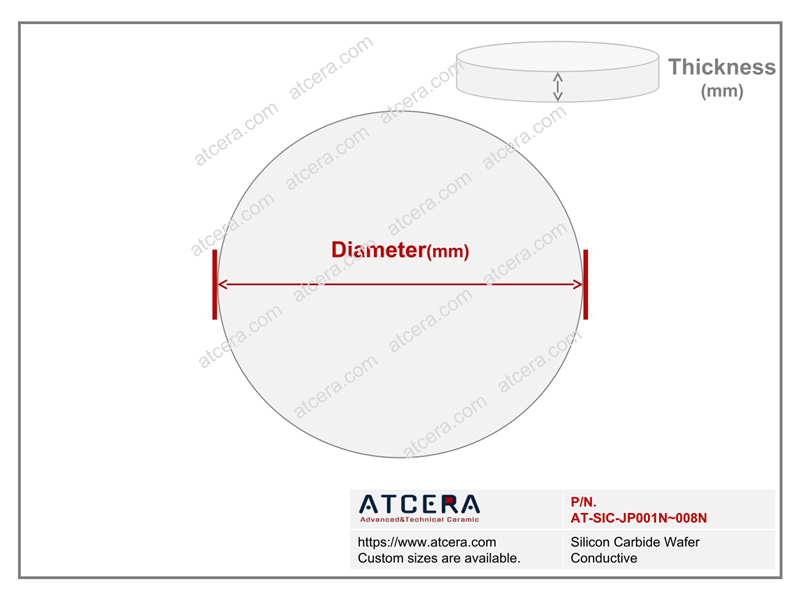
Silicon carbide wafers need to be cleaned before use to remove dirt and impurities on the surface.
 
1. Put the silicon carbide wafer into distilled water, soak for a period of time, and then gently wipe the surface with a soft cloth before taking it out;
 
2. Put in a chemical cleaning agent, soak for a period of time, and then take it out;
 
3. Take out the cleaned silicon carbide wafer, rinse the surface with water, then take it out and dry it;
 
4. In the cleaning process, avoid using too intense mechanical friction or high temperature heating, and ensure that the cleaning environment and tools are clean to avoid pollution.
 

Valuable Information


SiC Substrate Packing

SiC Substrate Packing


SiC substrates are carefully packaged in appropriate containers to avoid any potential damage.


Customization Advantages


1. According to your application scenario, analyze the needs, choose the appropriate material and processing plan.


2. Professional team, quick response, can provide solutions and quotations within 24 hours after confirming the demand.


3. Flexible business cooperation mechanism, support at least one piece of quantity customization.


4. Quickly provide samples and test reports to confirm that the product meets your needs.


5. Provide product use and maintenance suggestions to reduce your cost of use.

Related Blog
Preparation Of Aluminum Nitride Substrate And Selection Of Sintering Additives
In the field of high-tech materials, aluminum nitride (AlN) ceramics, with its excellent thermal conductivity, excellent electrical insulation properties and excellent mechanical strength, have become the core material in key fields such as electronic packaging, power electronics and microwave communication equipment. However, the preparation of aluminum nitride substrate is a complex process...
Application Requirements Of Aluminum Nitride Substrate
Aluminum nitride (AlN) as an advanced ceramic material, because of its unique physical and chemical properties, has shown great application potential in electronic packaging, power electronics, high frequency communication and other fields. As a core component in these fields, aluminum nitride substrates not only have to meet the basic physical performance requirements, but also need to ...
Effect Of Bulk Density Of Granulated Powder On Sintering Densification Of Silicon Nitride Balls
  Si3N4 powder is the main raw material for the preparation of silicon nitride balls. Selecting the appropriate treatment method to obtain the powder with regular shape and uniform particle size distribution is the basis for the stable implementation of Si3N4 ceramic ball forming, sintering, processing and other processes. According to the different atomization methods, the spray gr...
Optimizing The Spray Granulation Process To Improve The Performance Of Si3N4 balls
Silicon nitride (Si3N4) balls show great potential in the field of high-speed, high-precision, long-life bearings due to their excellent properties, such as lightweight, self-lubricating, high insulation, non-magnetic, high elastic modulus and excellent corrosion resistance. This paper aims to discuss the optimization of the spray granulation process of Si3N4 powder, especially the press...
Silicon Nitride Ball: A New Choice For High-Tech Powder Grinding Media
With the rapid development of high-tech industry, the requirements for fineness, purity and consistency of powder materials are increasing. As a key component in the powder preparation process, the performance of grinding medium directly determines the quality of the final product. Traditionally, zirconia ceramic balls are widely used in the field of ultra-fine grinding because of their high bendi...
Application Performance And Advantage Analysis Of Silicon Nitride Ball In Ultrafine Grinding Field
With the rapid development of nanotechnology and ultrafine material science, the demand for high-purity and ultrafine powder is increasing day by day. Silicon nitride ball, with its excellent hardness, very low wear rate and good chemical stability, has gradually become the key grinding medium in the field of ultrafine grinding. The purpose of this paper is to systematically describe the performan...
Study On Performance Characteristics And Application Of Silicon Nitride Ball In Mechanical Engineering Field
With the rapid development of modern mechanical engineering technology, the requirements for material properties are increasingly stringent, especially under extreme conditions such as high temperature, high speed, strong corrosion, etc., traditional metal materials and polymer materials have been difficult to meet the needs. Silicon nitride (Si ₄) As an advanced ceramic material with excellent ov...
Sol-gel Polishing Technology: Challenges And Opportunities To Innovate Silicon Carbide Substrate Polishing
Silicon carbide, the emerging star of the semiconductor material industry, is gradually leading the innovation trend of microelectronics technology with its excellent performance indicators. Its unique thermal conductivity, far superior to traditional semiconductor materials, provides the possibility for efficient heat dissipation, especially in high-power electronic devices show unparalleled adva...
Application And Advantages Of Plasma Assisted Polishing In AlN Substrate Processing
Aluminum nitride (AlN) ceramics, as a material with excellent thermal conductivity, mechanical properties and electrical properties, have been widely used in large-scale integrated circuits and electronic packages in recent years. Its excellent properties make it an ideal cooling substrate and packaging material. However, due to the high hardness, high brittleness and low fracture toughness of alu...
Silicon Carbide Substrate Processing Challenges with Innovative Applications Of Metal Friction-induced Reaction Grinding Technology
In the field of semiconductor materials, silicon carbide (SiC) with its excellent thermal conductivity, wide band gap characteristics, high breakdown electric field strength and high electron mobility, is gradually becoming a research and development hotspot, leading the innovation of a new generation of electronic devices. As a substrate material for key components, the broad application prospect...

Related Products

FAQ

Although our primary focus is on advanced ceramic materials such as alumina, zirconia, silicon carbide, silicon nitride, aluminum nitride, and quartz ceramics, we are always exploring new materials and technologies. If you have a specific material requirement, please contact us, and we will do our best to fulfill your needs or find suitable partners.

Absolutely. Our technical team possesses profound knowledge of ceramic materials and extensive experience in product design. We are happy to provide you with material selection advice and product design support to ensure optimal performance for your products.

We do not have a fixed minimum order value requirement. We always focus on meeting our customers' needs, and we strive to provide quality service and products regardless of the order size.

In addition to ceramic products, we also provide a range of additional services, including but not limited to: customized ceramic processing services based on your needs, using blanks or semi-finished blanks produced by yourself; if you are interested in outsourced ceramic packaging and metallization services, please contact us for further discussion. We are always committed to providing you with a one-stop solution to meet your various needs.

Yes, we do. No matter where you are located globally, we can ensure the safe and timely delivery of your order.

Send Your inquiry

Upload
* File ONLY PDF/JPG./PNG. Available.
Submit Now

Contact With Us

Contact With Us
Simply fill out the form below as best you can. And don't sweat the details.
Submit
Looking for Video?
Contact Us #
19311583352

Office Hours

  • Monday to Friday: 9:00 AM - 12:00 PM, 2:00 PM - 5:30 PM

Please note that our office hours are based on Beijing Time, which is eight hours ahead of Greenwich Mean Time (GMT). We appreciate your understanding and cooperation in scheduling your inquiries and meetings accordingly. For any urgent matters or queries outside our regular hours, feel free to contact us via email, and we will get back to you as soon as possible. Thank you for your business, and we look forward to serving you.

Home

Products

whatsApp

contact